AD9911DDS: Unterschied zwischen den Versionen
Aus LaborWiki
Siro (Diskussion | Beiträge) K (+pictures) |
Siro (Diskussion | Beiträge) K (+more details) |
||
| Zeile 27: | Zeile 27: | ||
* SDIO_0 MOSI | * SDIO_0 MOSI | ||
* SDIO_2 MISO | * SDIO_2 MISO | ||
* PLL 20x, 500MSPS DAC | |||
* maximum frequency possible 250Mhz | |||
* maximum frequency recommended 150Mhz | |||
* low pass required | |||
* active current 120mA | |||
* output AC coupled | |||
==== channels ==== | ==== channels ==== | ||
| Zeile 80: | Zeile 86: | ||
I've created a simple programm that runs on teensy 2.0 (ATMEGA32U4). It should run on any ATmega, just change the I/O ports.<br> | I've created a simple programm that runs on teensy 2.0 (ATMEGA32U4). It should run on any ATmega, just change the I/O ports.<br> | ||
Timings are not critical, as the ATmega is much slower than the maximum I/O updaterate of the AD9911. | Timings are not critical, as the ATmega is much slower than the maximum I/O updaterate of the AD9911. | ||
<br> | |||
Software flow: | |||
* write register 0 (channel select bits) | |||
* write register 1 and 2 (digital power down, pll multiplier) | |||
* write to selected channel registers 0x03 - 0x18 | |||
* toogle I/O-Update pin | |||
*TODO upload files* | *TODO upload files* | ||
Version vom 24. Dezember 2013, 11:43 Uhr
| AD9911DDS Release status: experimental [box doku] | |
|---|---|

| |
| Description | Direct Digital Synthesizer |
| Author(s) | siro |
| Last Version | 0.1 |
| Platform | * |
| License | GPL |
AD9911DDS
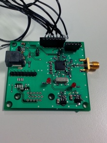
This project describes the AD9911 Direct Digital Synthesizer. It is capable of generating a sine-wave between 250Mhz and >1Hz. The created evaluation unit is descripted here.
The Hardware
- CLK_MODE_SEL = 1.8V
- Rset = 1k91
- crystal 25Mhz
- DVDD 1.8V
- AVDD 1.8V
- DVIO 3.3V
- SDIO_0 MOSI
- SDIO_2 MISO
- PLL 20x, 500MSPS DAC
- maximum frequency possible 250Mhz
- maximum frequency recommended 150Mhz
- low pass required
- active current 120mA
- output AC coupled
channels
There are four channels:
- channel 0: aux channel
- channel 1: primary channel
- channel 2: aux channel
- channel 3: aux channel
channel 1 is connected to the DAC. all aux channels are capable of modulating channel 1.
modes of operation
- single tone (frequency,amplitude,phase adjustable)
- 2 tone test mode (amplitude modulated single tone)
- 2/4/8/16 FSK/ASK/PSK
- frequency/amplitude/phase ramp up
- frequency/amplitude/phase ramp down
- frequency/amplitude/phase sweep
SPI interface
default
2-wire SPI mode, SDIO_0 is bidirectional !
- SPI write
- CPOL=0
- CPHA=0
- SPI read
- CPOL=1
- CPHA=1
3-wire SPI mode
- configure 3-wire SPI mode using reg 0
- set msb mode (default) using reg 0
- SDIO_0 is MOSI
- SDIO_2 is MISO
MSB/LSB mode
- MSB
- the Most Significant Bit is transfered first
- the Most Significant Byte is transfered first
- LSB
- the Least Significant Bit is transfered first
- the Least Significant Byte is transfered first
register select
- register 0, 1, 2 are independent
- channel register 0x03 - 0x18 are written to using the enable bits in register 0
- you can write to multiple channels at once !
*TODO upload files*
The Software
I've created a simple programm that runs on teensy 2.0 (ATMEGA32U4). It should run on any ATmega, just change the I/O ports.
Timings are not critical, as the ATmega is much slower than the maximum I/O updaterate of the AD9911.
Software flow:
- write register 0 (channel select bits)
- write register 1 and 2 (digital power down, pll multiplier)
- write to selected channel registers 0x03 - 0x18
- toogle I/O-Update pin
*TODO upload files*
Changes applied to Hardware
- pull PWR_DWN_CTL low
- pull SDIO_3 low
- terminate IDAC with 50 Ohms agains AVCC
- terminate !IDAC with 50 Ohms agains AVCC
- include a 5th order low pass filter
- include a transformer
- series resistance for SPI interface
